 1/1
1/1
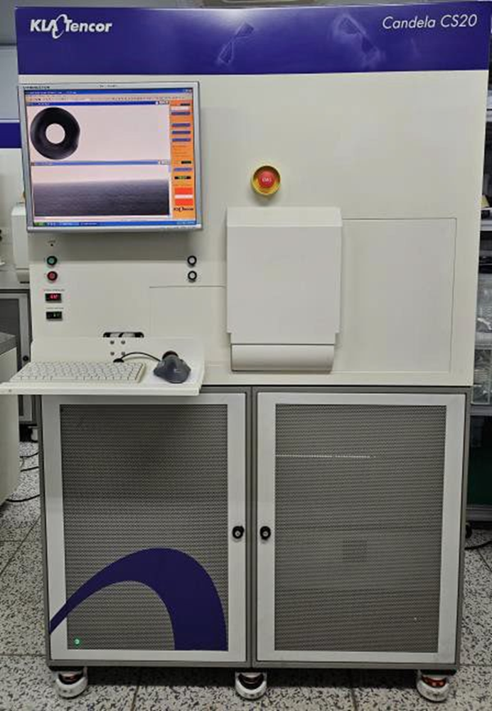
KLA-Tencor Candela CS20
ASIA (North East)
Wafer Size 8"
Vintage 2010-6
Tool's Condition Excellent
[ General Description ]
Wafer Size : 2 ~8 inch
Illumination Source : 8mW laser, 635 nm wavelength
Operator Interface : Trackball and keyboard standard
Substrate Thickness : 350 μm ~ 1,100 μm
Substrate Material : Any clear or opaque polished surface
[ Performance ]
Defect Sensitivity 0.08 μm diameter
PSL sphere equivalent > 95% capture rate(PSL on bare Si)
Other Defects and Applications : Particles, scratches, stains, pits, and bumps.
Sensitivity: Minimum detectable size for automatic defect classification:
- Scratches: 100 μm long, 0.1 μm wide, 50 Å;; deep.
- Pits: 20 μm diameter, 50 Å;; deep
- Stains: 20 μm diameter, 10 Å;; thick
[ Application ]
- Opaque substrates
- EPI Layers
- Transparent film coatings (SiC, GaN, Sapphire)
*. Fully refurbished. Installed in Clean-room. Possible demo anytime.